

Semiconductor Carrier Tape for IC Packaging | Design, Materials & Applications
What Is Semiconductor Carrier Tape for IC Packaging?
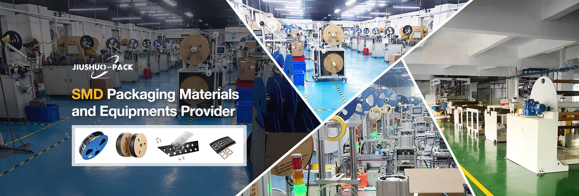
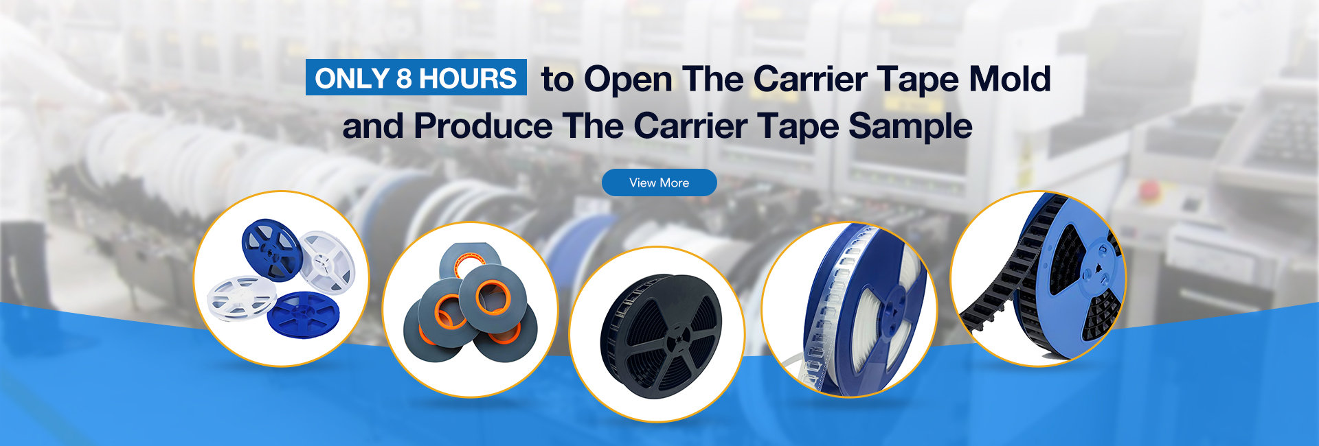
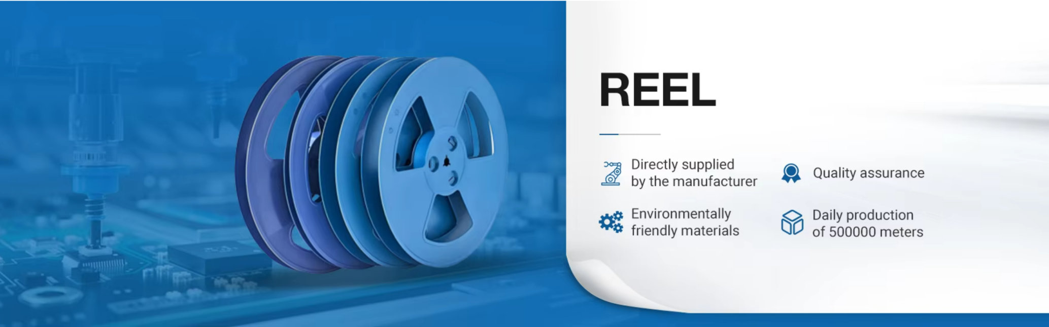
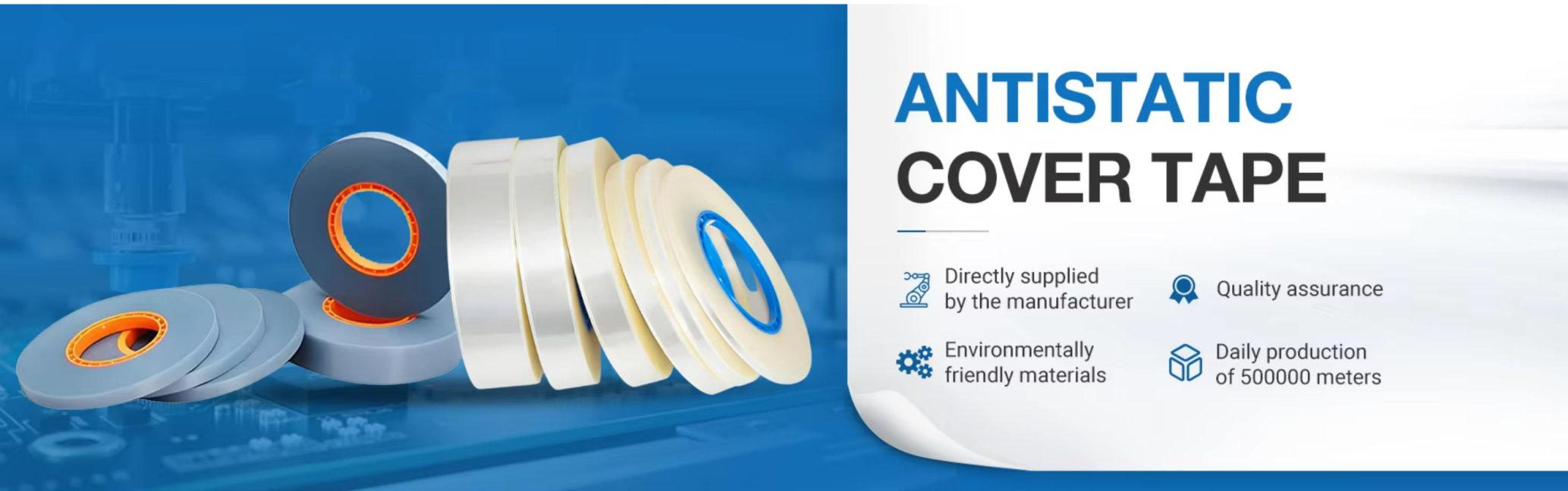
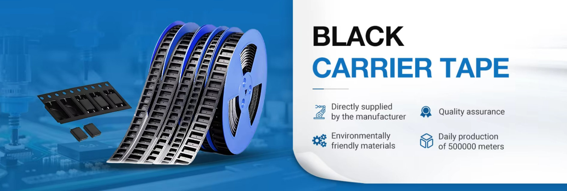
Semiconductor carrier tape is a crucial component used in the packaging of integrated circuits (ICs) for semiconductor manufacturing. It is designed to safely carry and protect semiconductor components, such as microchips and other sensitive electronic parts, during the Surface-Mount Technology (SMT) assembly process. The carrier tape typically consists of three main components: the carrier tape itself, the cover tape, and the reel, forming a complete packaging solution.
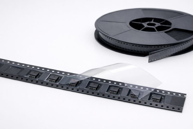
The carrier tape holds the IC components securely in place, ensuring their proper alignment and preventing any damage during handling and transportation. Key features of the carrier tape include the D1 hole, pockets, and pitch, which are carefully engineered to match the precise dimensions required for various IC packages. These features are vital to maintaining the integrity and reliability of the components throughout the entire manufacturing process.
Why Semiconductor Carrier Tape Is Essential for IC Packaging
The need for semiconductor carrier tape in IC packaging cannot be overstated, especially in the context of modern, high-precision manufacturing. Semiconductor components are extremely small, thin, and fragile, which makes them prone to damage during handling, transportation, or insertion into pick-and-place machines.
Carrier tape provides the necessary stability and protection to these sensitive ICs by securely holding them in place during the assembly process. It ensures that the components are delivered accurately to the pick-and-place machines, maintaining alignment and minimizing the risk of misplacement or damage. The use of carrier tape helps maintain the integrity of the semiconductor components, ensuring that they remain intact from storage through to the final stages of packaging.
Additionally, the accurate delivery of IC components in carrier tape plays a critical role in optimizing production efficiency and throughput, ultimately leading to higher yields and reduced costs. Without the use of specialized carrier tapes, the handling and placement of such delicate components would become far more error-prone, impacting both quality and production timelines.
Key Design Considerations for Semiconductor Carrier Tape
When designing semiconductor carrier tape, several key factors must be taken into account to ensure compatibility and efficiency in IC packaging. These considerations directly impact the accuracy, reliability, and overall success of the packaging process.
-
Pocket Size & Depth: The size and depth of the pockets on the carrier tape are closely linked to the IC package dimensions. These parameters must be carefully designed to ensure a secure fit for each semiconductor component, preventing movement or damage during transportation. Incorrect pocket sizes could result in components being misaligned or even crushed.
-
Pitch Selection: The pitch, or the distance between each pocket on the carrier tape, plays a significant role in the alignment and precision of the components during placement. A consistent and appropriate pitch ensures that the components are fed accurately into the pick-and-place machine, enhancing both efficiency and the precision of the manufacturing process.
-
Material Choice: The choice of material for the carrier tape is critical, as it must meet specific requirements depending on the type of IC being packaged. Materials like polycarbonate (PC), polystyrene (PS), or polyester (PET) are commonly used. Additionally, for ICs that are sensitive to electrostatic discharge (ESD), conductive or anti-static materials are often preferred to protect the components from potential damage.
-
D1 Hole & Feeder Indexing Precision: The D1 hole is a small but crucial feature in carrier tape design. It allows the feeder system to index and align the tape precisely during the SMT process. The accuracy of the D1 hole and its alignment with the feeder indexing mechanism is vital for smooth operation and reliable component placement.
While all these factors contribute to the overall performance of the semiconductor carrier tape, it is important to note that stability and accuracy are more crucial than simply adhering to dimensional specifications. A well-designed carrier tape must prioritize consistency and reliable performance over rigid adherence to size alone.
Materials for Semiconductor Carrier Tape
The material choice for semiconductor carrier tape is critical, as it directly influences the performance, reliability, and safety of IC packaging. The materials selected must meet stringent criteria to ensure the secure transport and protection of semiconductor components throughout the entire manufacturing process.
-
Conductive Materials: One of the most common material choices for semiconductor carrier tape is conductive material. This is particularly important for ICs that are sensitive to electrostatic discharge (ESD). Conductive materials, such as antistatic polycarbonate (PC), or even specialized conductive plastics, help to dissipate static charges, protecting the delicate semiconductor components from ESD damage. This is crucial in preventing component failure during the pick-and-place operation or other assembly processes.
-
Polycarbonate (PC): Polycarbonate is a popular choice for semiconductor carrier tape because of its strength, clarity, and ease of use in precision manufacturing. It is often chosen for its durability and resistance to environmental factors such as moisture and temperature fluctuations, ensuring that the ICs remain securely positioned during transportation and handling.
-
Polystyrene (PS): Polystyrene is another material commonly used in the production of carrier tapes. It offers a balance of low cost and good performance. While not as resistant to impact or temperature fluctuations as polycarbonate, it is still a viable option for less sensitive components.
-
Polyester (PET): Polyester is frequently used in carrier tapes for its excellent chemical resistance, strength, and flexibility. It is particularly suitable for lightweight components, providing secure and stable handling. PET is also widely chosen for its cost-effectiveness and ease of processing.
-
Electrostatic Discharge (ESD) Materials: For components requiring stringent electrostatic protection, conductive materials designed to prevent the buildup of static charges are used. These materials are often incorporated into the carrier tape‘s design to ensure safe handling and transportation of the most sensitive semiconductor components, such as memory chips, processors, and other high-precision parts.
The selection of the right material depends largely on the specific IC package being handled, the level of sensitivity to electrostatic discharge, and environmental factors such as humidity or temperature. Manufacturers must carefully evaluate these variables to determine the optimal material for their carrier tape design.
Applications of Semiconductor Carrier Tape in IC Packaging
Semiconductor carrier tape is widely used across multiple IC packaging and semiconductor-related applications where precision, protection, and process stability are critical. Its role extends beyond simple transportation, directly supporting automated handling and high-yield production.
In IC packaging, carrier tape is engineered to accommodate a wide range of semiconductor packages, including logic ICs, memory devices, and other miniaturized components. The pocket geometry is designed to control orientation and limit movement, ensuring each IC remains stable during storage, shipping, and SMT feeding. This stability is essential for maintaining placement accuracy in high-speed pick-and-place operations.
In LED packaging, similar carrier tape principles are applied to handle light-emitting semiconductor devices. LEDs often require consistent orientation and protection from mechanical stress, making tape-and-reel packaging a practical and reliable solution.
Carrier tape is also commonly used for ESD-sensitive and environmentally sensitive components, where exposure to static electricity, humidity, or temperature variation can affect performance. In these cases, carrier tape helps create a controlled packaging environment that supports safe handling throughout the supply chain.
Across these applications, semiconductor carrier tape functions as a standardized interface between component packaging and automated assembly, enabling efficient, repeatable, and scalable IC production without referencing specific brands or device models.
How Semiconductor Carrier Tape Works in IC Packaging
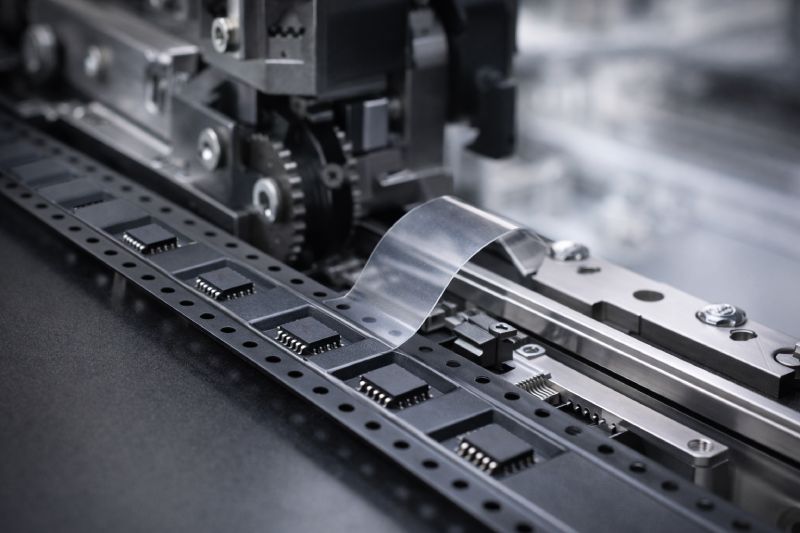
In IC packaging and SMT production, semiconductor carrier tape functions as the physical interface between packaged components and automated assembly equipment. Its primary role is to ensure that each IC is delivered to the pick-and-place system in a controlled, repeatable, and damage-free manner.
During packaging, semiconductor components are placed into precisely formed pockets within the carrier tape. Each pocket controls the component’s position and orientation, while the pitch ensures consistent spacing between adjacent ICs. A cover tape is then sealed over the carrier tape, securing the components in place and preventing movement during transport and storage.
When the tape-and-reel package enters the SMT production line, the feeder mechanism engages with the D1 holes along the tape edge. These holes allow the feeder to index the tape accurately, advancing one pocket at a time to the pick-up position. As the cover tape is peeled back at a controlled angle, individual ICs are exposed exactly where the pick-and-place nozzle expects them.
This coordinated interaction between carrier tape geometry, feeder indexing, and cover tape peeling is what enables high-speed placement without shifting, flipping, or damaging delicate semiconductor components.
Common Issues in Semiconductor Carrier Tape Packaging
Despite its critical role in IC packaging, semiconductor carrier tape packaging can introduce risks if design, material selection, or process control is insufficient. These issues often surface during high-speed SMT operations, where tolerances are tight and stability is essential.
One common issue is pocket deformation or misalignment. If pocket geometry lacks sufficient rigidity or consistency, semiconductor components may tilt, rotate, or sit unevenly. This can lead to pick-up failures or incorrect placement during assembly, especially for thin or fine-pitch IC packages.
Another frequent risk is feeder mismatch or feeding instability. Inaccurate D1 hole positioning, inconsistent pitch, or dimensional variation along the tape length can cause poor engagement with feeder indexing mechanisms. This may result in skipped pockets, double feeding, or intermittent stoppages on the production line.
Inconsistent component alignment is also a concern, particularly when pocket tolerances are not well matched to the IC package. Even minor shifts in orientation can reduce placement accuracy and increase the likelihood of defects downstream.
These issues do not always cause immediate failures but can gradually impact yield, throughput, and overall process reliability, making carrier tape packaging a critical risk point in semiconductor manufacturing workflows.
When Custom Semiconductor Carrier Tape Is Required
Standard semiconductor carrier tape designs are suitable for many IC packaging scenarios, but certain production conditions demand a custom solution. Recognizing when customization is necessary is critical for maintaining placement accuracy, yield, and overall process stability.
Custom semiconductor carrier tape is often required for non-standard IC packages. Components with unique outlines, uncommon thicknesses, asymmetric shapes, or special orientation requirements may not fit securely into standard pocket designs. In these cases, a custom pocket geometry is needed to control movement and ensure consistent positioning.
High-speed or high-precision production lines also increase the need for custom carrier tape. As placement speeds rise and tolerances tighten, even small variations in pocket shape, pitch, or material behavior can affect feeding stability. Custom designs allow tighter control over these variables, supporting reliable feeder engagement and accurate pick-up.
Customization is particularly important in yield-critical processes, where component damage, misfeeds, or placement errors have a direct impact on production efficiency and cost. By tailoring pocket design, material selection, and tape geometry to the specific IC and production environment, manufacturers can reduce risk at these sensitive stages.
Standards and Compatibility in Semiconductor Carrier Tape Packaging
Standards play a key role in ensuring semiconductor carrier tape works reliably across different packaging, transport, and SMT assembly environments. Among these, EIA-481 is the most widely referenced standard for tape-and-reel packaging, defining critical parameters such as pocket dimensions, pitch, tape width, and D1 hole positioning.
In semiconductor packaging, adherence to EIA-481 helps ensure cross-equipment compatibility. Carrier tape designed within standard tolerances can run consistently across feeders, pick-and-place machines, and inspection systems from different equipment manufacturers, reducing integration risks when production lines change or expand.
At the same time, standardization does not eliminate the need for non-standard or semi-custom designs. Many IC packages fall outside typical dimensional ranges, requiring custom pocket geometry while still aligning with EIA-481 indexing and interface rules. This balance allows manufacturers to maintain feeder compatibility without compromising component stability.
By following internationally recognized standards while allowing controlled customization, semiconductor carrier tape packaging achieves both flexibility and reliability—supporting stable production across global supply chains.
Summary
Semiconductor carrier tape plays a fundamental role in IC packaging by providing a stable, precise, and repeatable way to handle delicate semiconductor components throughout storage, transport, and SMT assembly. From pocket design and material selection to feeder compatibility and standard compliance, each aspect of the carrier tape directly affects placement accuracy and production yield.
Across IC packaging applications, carrier tape functions as more than protective packaging—it acts as a critical interface between semiconductor components and automated manufacturing equipment. When standard designs are insufficient, custom semiconductor carrier tape enables tighter control over high-precision and yield-sensitive processes.



 Emial
Emial John Mr