
IC Carrier Tape for SMT & Semiconductor Assembly
What Is IC Carrier Tape for SMT & Semiconductor?
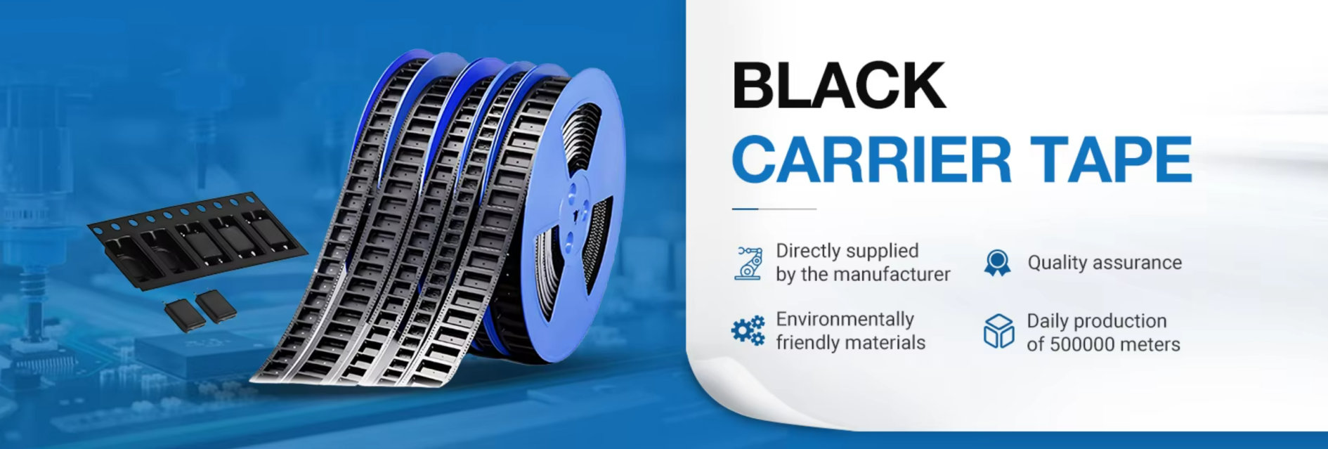
IC carrier tape is a component-specific packaging solution designed for integrated circuits (ICs) used in SMT assembly and semiconductor-related automated processes. It holds ICs in precisely formed pockets and advances them at a controlled pitch, with standardized sprocket holes ensuring accurate indexing during feeding.
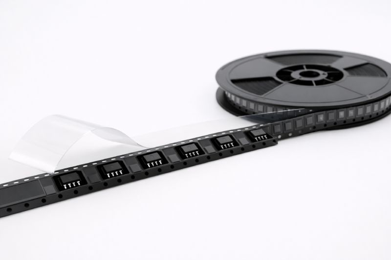
In practice, the role of IC carrier tape is not simply to “contain” ICs, but to present each device to automated equipment in a stable, repeatable, and predictable manner. During transport, storage, and machine loading, the tape maintains consistent orientation, minimizes movement, and protects delicate leads or pads from mechanical stress.
Within high-speed pick-and-place systems and post-packaging semiconductor workflows, carrier tape acts as the critical interface between the IC and automation equipment. As a result, IC carrier tape is best understood as an engineering-driven packaging component, optimized for feeding reliability, positional accuracy, and device protection rather than general packaging convenience.
Why ICs Require Specialized Carrier Tape
Integrated circuits place much higher demands on carrier tape than most passive components. ICs are typically smaller, lighter, and more structurally complex, with exposed leads, solder pads, or delicate package edges that are easily damaged by movement or misalignment. Even minor instability during feeding can result in bent leads, pad contamination, or placement errors.
In addition, ICs require strict orientation control. A slight rotation inside the pocket can cause pick-and-place nozzles to miss the target or place the device incorrectly, especially at high speeds. This makes pocket geometry, depth control, and pitch consistency far more critical than in standard tape-and-reel applications.
Just as important is repeatability. SMT and semiconductor equipment rely on predictable indexing cycles, where each IC must appear in the exact same position every time. Generic carrier tape designed for passive components cannot consistently meet these requirements.
Typical IC Packages Used with Carrier Tape
IC carrier tape is used across a wide range of IC package types, each with different structural characteristics that directly influence pocket design. For leadframe-based packages such as QFN, QFP, SOP, and SOIC, the tape must control both vertical support and lateral restraint. Leads or exposed pads must remain protected while ensuring the package sits flat and can be reliably picked from the pocket.
For array-style packages such as BGA and LGA, the focus shifts from lead protection to planarity and underside clearance. These packages often require carefully managed pocket depth and bottom support to prevent solder ball contact or deformation during feeding and transport.
In addition, many projects involve custom or application-specific IC packages, including miniaturized designs, asymmetric outlines, or non-standard thicknesses. These ICs rarely fit well in off-the-shelf carrier tape and demand tailored pocket geometry to control orientation and movement.
Across all package types, the key point is that different IC structures impose different mechanical constraints. As a result, carrier tape for ICs is never a one-size-fits-all solution—pocket shape, support points, and retention logic must be adapted to the specific package form to ensure stable, repeatable automation.
Key Design Factors for IC Carrier Tape
The performance of IC carrier tape is largely determined by how well its design aligns with the mechanical and process requirements of automated equipment. Pocket geometry and depth are the first critical factors. The pocket must securely hold the IC without excessive clearance, while still allowing smooth release during pick-and-place. Too shallow, and the IC may shift or rotate; too deep, and vacuum pickup reliability can be affected.
Pitch consistency directly influences feeding rhythm. In SMT systems, even small pitch deviations can accumulate over long runs, leading to indexing errors or misalignment at the pickup point. For ICs running at high placement speeds, stable and repeatable pitch is essential for maintaining throughput and yield.
Another key element is the D1 sprocket hole, which defines how accurately the tape advances through feeders. Precise alignment between the D1 hole and pocket center ensures that each IC arrives at the correct position relative to the pickup nozzle. Poor D1 hole control often results in inconsistent placement or intermittent feeding issues.
Finally, dimensional tolerance control ties all design elements together. IC carrier tape operates within tight mechanical margins, especially in high-speed SMT environments. Variations in pocket size, hole position, or tape thickness can quickly translate into feeding instability or placement defects.
In short, IC carrier tape design is a balance between secure retention, predictable release, and precise indexing—each factor reinforcing the others to support reliable, repeatable automation.
Materials Used for IC Carrier Tape
Material selection plays a decisive role in how IC carrier tape performs during forming, feeding, and long-term use. Common materials include PC (polycarbonate), PS (polystyrene), and PET, each offering different balances of stiffness, formability, and dimensional stability. For IC applications, the material must support precise pocket formation while maintaining consistent geometry under mechanical stress.
PC is often chosen for high-precision or demanding IC applications due to its strength and thermal stability, which help maintain pocket accuracy during high-speed SMT feeding. PS offers good formability and cost efficiency, making it suitable for many standard IC packages when extreme tolerance control is not required. PET provides a balance between rigidity and flexibility, with improved crack resistance in certain environments.
Beyond base polymers, conductive and ESD-safe materials are especially important for ICs. Integrated circuits are highly sensitive to electrostatic discharge, and uncontrolled static buildup during transport or feeding can compromise device reliability. Conductive carrier tape helps dissipate charge and reduce ESD risk throughout the handling process.
Ultimately, the right material supports not only IC protection, but also consistent forming accuracy and stable feeding behavior across the entire SMT or semiconductor workflow.
IC Carrier Tape in SMT Assembly
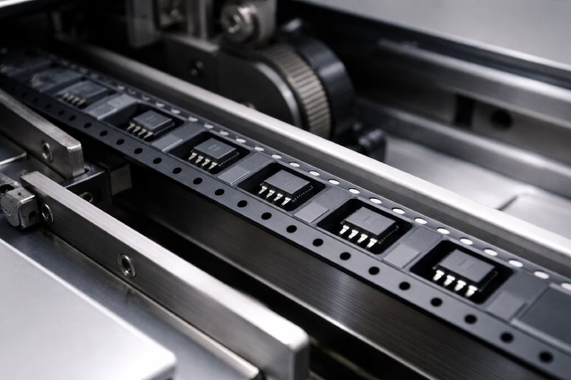
In SMT assembly, IC carrier tape serves as the primary delivery format that enables automated pick-and-place operations. The tape feeds through the SMT feeder, advancing each IC to a fixed pickup position where vacuum nozzles retrieve the component and place it onto the PCB. Throughout this process, feeding stability and positional repeatability are critical.
ICs are often placed at high speeds and with tight placement tolerances. Any variation in pocket position, tape flatness, or indexing accuracy can lead to missed picks, skewed placement, or machine stoppages. Compared with passive components, ICs are far less forgiving of such inconsistencies due to their size, weight, and package geometry.
High-speed SMT lines place additional demands on IC carrier tape. The tape must maintain dimensional stability under continuous motion, while pockets must release ICs cleanly without sticking or tipping. As a result, IC carrier tape used in SMT is engineered not just for compatibility, but for process reliability under sustained, high-throughput conditions.
IC Carrier Tape in Semiconductor and Packaging Processes
Beyond SMT assembly, IC carrier tape is also widely used in semiconductor and post-packaging processes. After ICs are packaged, they often pass through automated steps such as testing, inspection, sorting, and final preparation for shipment. In these stages, carrier tape provides a controlled and standardized method of handling large volumes of devices without manual contact.
Compared with SMT-focused tape, semiconductor applications often place higher emphasis on precision and protection. ICs may be more sensitive to mechanical shock, contamination, or electrostatic discharge, requiring tighter pocket tolerances and more stable materials. In some cases, carrier tape must support longer dwell times in storage or repeated handling cycles before final use.
It is also important to distinguish IC carrier tape from broader semiconductor carrier tape categories. While the two overlap, IC-specific tape is typically optimized for downstream automation compatibility, whereas semiconductor carrier tape may be designed to meet stricter handling or environmental requirements earlier in the supply chain.
For certain IC projects—especially those involving advanced packaging or high-value devices—higher-specification carrier tape becomes a necessary part of maintaining yield and reliability.
Common Issues with IC Carrier Tape
Problems with IC carrier tape often become visible only after automation begins. One common issue is IC rotation inside the pocket, which can occur when pocket geometry does not adequately control lateral movement. Even slight rotation may cause pickup failures or incorrect placement, particularly in high-speed SMT lines.
Another frequent concern is pocket deformation. Inconsistent forming, unsuitable material selection, or excessive mechanical stress during feeding can cause pockets to lose their intended shape. This may lead to unstable IC seating or difficulty during release at the pickup point.
Feeding instability is also a recurring risk. Variations in pitch accuracy, tape flatness, or sprocket hole alignment can disrupt indexing, resulting in misfeeds or intermittent machine stops. These issues tend to compound over long production runs.
Finally, ESD exposure remains a critical but sometimes overlooked risk. If the carrier tape material does not properly dissipate static charge, ICs may be exposed to electrostatic stress during transport or feeding, potentially affecting device performance or long-term reliability.
When Custom IC Carrier Tape Is Required
Standard IC carrier tape works well for many common packages, but there are clear situations where custom carrier tape becomes necessary. One typical trigger is a non-standard IC package—for example, unusual outlines, asymmetric shapes, atypical thickness, or custom lead configurations. These ICs often cannot be held securely or oriented correctly using off-the-shelf pocket designs.
Custom tape is also frequently required in high-speed SMT or high-yield production environments. As placement speeds increase, tolerance margins shrink. Even small compromises in pocket fit or pitch accuracy can lead to feeding instability or placement errors, making a tailored design essential for process reliability.
Another common case involves ICs with special structural or handling requirements, such as exposed pads, fragile leads, or sensitivity to movement and shock. In these situations, custom pocket geometry is used to control contact points and retention behavior more precisely.
Rather than being a last resort, custom IC carrier tape is often a proactive engineering choice—used to align packaging design with specific IC characteristics and process demands.
Summary
IC carrier tape plays a critical dual role across both SMT assembly and semiconductor-related processes. At the component level, it is not simply a packaging format, but an engineering interface that ensures ICs are protected, correctly oriented, and consistently presented to automated equipment.
For SMT engineers, IC carrier tape directly affects feeding stability, placement accuracy, and line efficiency. For semiconductor and packaging teams, it supports safe handling, precision control, and reliable downstream automation. Across both contexts, pocket design, pitch accuracy, material selection, and tolerance control determine whether ICs move smoothly through high-speed processes—or introduce risk.
Understanding when standard tape is sufficient and when custom IC carrier tape is required is a key decision point for maintaining yield and process stability.



 Emial
Emial John Mr