


WLCSP Carrier Tape Design Guide: Materials, Tolerance & SMT Challenges
What Is WLCSP and Why Packaging Is Challenging
Wafer Level Chip Scale Package (WLCSP) is a semiconductor packaging technology in which the final package size is nearly identical to the silicon die itself. Instead of adding a traditional protective package after wafer fabrication, the interconnect structure—typically solder balls—is formed directly on the wafer before the chips are singulated. This wafer-level manufacturing approach enables extremely compact devices with very high I/O density, making WLCSP widely used in smartphones, wearables, and other space-constrained electronics.
However, these advantages also introduce significant packaging challenges. Because there is no protective molded body, WLCSP components rely on exposed solder balls for electrical and mechanical connection. These solder balls are highly fragile and susceptible to deformation, contamination, or damage during handling and transport.
In addition, the extremely small package size requires precise orientation control and very high pick-and-place accuracy during SMT assembly. Even minor positional deviations can cause misalignment during placement.
As a result, many standard electronic packaging methods struggle to reliably handle WLCSP devices without specialized design considerations.
Why Carrier Tape Is Used for WLCSP Packaging
Carrier tape packaging has become the most widely used method for handling and transporting WLCSP components in modern SMT production. In high-volume electronics manufacturing, components must be delivered to pick-and-place machines in a format that supports continuous, automated feeding. Tape & reel packaging provides this capability by organizing components in a precisely spaced pocket structure that aligns with SMT feeder indexing.
One of the main advantages of carrier tape is its compatibility with high-speed automated assembly lines. Components stored in the tape pockets are protected during transportation while remaining correctly oriented for vacuum pickup during SMT placement. The sealed structure—formed by carrier tape and cover tape—also helps reduce the risk of contamination or mechanical damage to delicate solder balls.
Alternative packaging formats such as tray packaging or waffle packs are sometimes used for semiconductor devices, but they are generally less efficient for large-scale SMT operations. Trays require manual loading or robotic transfer, and waffle packs are often limited to lower throughput environments.
For these reasons, carrier tape has become the most common feeding format for WLCSP components in automated SMT assembly processes.
Key Design Challenges for WLCSP Carrier Tape
Designing carrier tape for WLCSP components is significantly more demanding than for conventional packaged ICs. Because WLCSP devices have exposed solder balls and extremely small dimensions, the tape pocket design must achieve very high precision while still ensuring reliable feeding during SMT assembly.
Pocket Geometry Precision
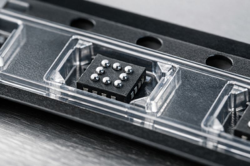
Pocket geometry is one of the most critical aspects of WLCSP carrier tape design. The pocket dimensions must maintain extremely tight tolerances to prevent excessive movement inside the cavity. At the same time, the pocket clearance must be carefully controlled so that the solder balls are not compressed or damaged.
Even minimal dimensional deviations can cause components to tilt, shift, or become unstable during feeder indexing. Therefore, WLCSP pockets are typically designed with minimal clearance and carefully engineered support surfaces that protect the solder balls while stabilizing the chip body.
Anti-Rotation Control
WLCSP components are particularly prone to rotation because their body shape is often symmetrical and extremely lightweight. If a component rotates inside the pocket, the pick-and-place machine may fail to recognize the correct orientation, leading to placement errors.
To prevent rotation, carrier tape designers often incorporate structural features such as corner supports or asymmetrical pocket geometry. These features help stabilize the device and ensure that the chip remains in a consistent orientation during transportation and SMT feeding.
Depth Control
Pocket depth must also be precisely matched to the component structure. If the pocket is too shallow, the solder balls may contact the pocket base and become damaged. If the pocket is too deep, the vacuum nozzle may struggle to reach the correct pickup height.
Designers must therefore balance pocket depth with the height of the solder balls and the thickness of the chip body to ensure safe storage and reliable pickup during SMT assembly.
Surface Protection
Finally, surface protection is a key consideration for WLCSP carrier tape. Since the solder balls serve as the electrical interface, any contamination, abrasion, or compression can negatively affect solder joint reliability. Smooth pocket surfaces and carefully controlled forming processes are required to prevent particle contamination or mechanical stress on the solder balls during packaging and transport.
Material Selection for WLCSP Carrier Tape
Material selection plays a crucial role in the performance and reliability of carrier tape used for WLCSP packaging. Because WLCSP components are extremely small and sensitive to dimensional variation, the tape material must provide high rigidity, stable pocket geometry, and consistent forming accuracy.
Three materials are commonly used in carrier tape manufacturing: polycarbonate (PC), polystyrene (PS), and polyethylene terephthalate (PET). Each material offers different mechanical and processing characteristics.
PC carrier tape is widely used for semiconductor applications due to its excellent rigidity and dimensional stability. During thermoforming, PC maintains precise pocket geometry and resists deformation under mechanical stress. This stability is particularly important for WLCSP devices, where even slight pocket deformation can affect pick-and-place accuracy. For a deeper overview of this material, see PC Carrier Tape.
PS carrier tape is commonly used for standard SMT components because it is cost-effective and easy to form. However, PS has lower mechanical strength and dimensional stability compared with PC, making it less suitable for extremely small or sensitive devices such as WLCSP.
PET carrier tape offers good transparency and moderate strength, but its forming precision can vary depending on the manufacturing process. In many semiconductor packaging applications, PET is used only when specific optical or material properties are required.
Overall, PC carrier tape is often preferred for WLCSP packaging because its rigidity and dimensional stability support the tight tolerances required for reliable SMT feeding. For a broader comparison of carrier tape materials, refer to the Carrier Tape Materials Guide.
Tolerance Requirements for WLCSP Carrier Tape
Tolerance control is one of the most critical engineering factors in WLCSP carrier tape design. Because WLCSP devices are extremely small and rely on exposed solder balls for electrical connection, even very small dimensional deviations in the carrier tape can directly affect pick-and-place accuracy during SMT assembly.
One key parameter is pocket tolerance. The pocket width, length, and depth must be controlled with extremely high precision to ensure that the component sits securely while still allowing the vacuum nozzle to access the pickup surface. If the pocket clearance is too large, the component may shift or tilt during feeder indexing. If it is too tight, the chip or solder balls may experience mechanical stress.
Another important factor is pitch accuracy. Carrier tape pockets must be positioned at consistent intervals so that the feeder mechanism can index the tape precisely. Even small pitch deviations can cause the pickup position to drift over multiple indexing steps. A detailed explanation of this parameter can be found in Carrier Tape Pitch Explained.
In WLCSP packaging, cumulative tolerance stack-up must also be considered. Variations from pocket dimensions, pitch spacing, feeder positioning, and pick-and-place calibration can combine to create significant placement errors. In practice, a deviation of only 0.02–0.05 mm may already affect pickup accuracy or cause alignment issues during SMT assembly.
For this reason, strict dimensional control and precision forming processes are required when producing carrier tape for WLCSP devices. More detailed tolerance principles are discussed in Carrier Tape Tolerance Explained.
Cover Tape Considerations for WLCSP Packaging
Cover tape plays a critical role in maintaining component stability and protecting WLCSP devices during transportation and SMT feeding. Because WLCSP components are extremely lightweight and sensitive to mechanical disturbance, the interaction between the cover tape and carrier tape must be carefully controlled.
One of the most important parameters is peel force. If the peel force is too high, the force generated during cover tape removal can cause components to shift, bounce, or even jump out of the pocket. This risk is particularly significant for WLCSP packages due to their small mass and exposed solder balls.
Another potential issue is vacuum pick interference. Inconsistent or unstable peeling behavior may create slight movement of the component just before the pick-and-place nozzle engages. This can reduce pickup accuracy and increase placement errors during high-speed SMT assembly.
To prevent these issues, the cover tape must provide stable and controlled peel force throughout the entire reel. Compatibility between the cover tape adhesive system and the carrier tape material is also essential to ensure consistent peeling performance.
Selecting the correct cover tape system is therefore a key part of reliable WLCSP packaging. More details about compatibility and selection criteria can be found in Cover Tape for Carrier Tape.
SMT Feeding Challenges for WLCSP Carrier Tape
SMT assembly of WLCSP components places extremely high demands on the entire feeding and placement system. Because these devices are very small and lightweight, even minor disturbances during feeding can lead to placement errors or component loss.

One of the primary challenges is pick-and-place accuracy. The vacuum nozzle must align precisely with the center of the component while avoiding contact with the fragile solder balls. If the component shifts slightly inside the pocket, the nozzle may fail to pick the device correctly or apply uneven force during pickup.
Feeder indexing stability is another important factor. As the feeder advances the carrier tape step by step, mechanical vibrations or inconsistent tape tension can cause components to move within the pocket. With larger packaged components this movement is usually tolerable, but WLCSP devices have very limited tolerance for positional deviation.
Additionally, component flipping or tilting may occur if the pocket geometry or depth is not properly designed. Once a component flips inside the pocket, the SMT machine cannot reliably detect or place it.
For these reasons, WLCSP packaging requires tighter coordination between carrier tape design, feeder precision, and pick-and-place calibration than most conventional SMT components.
When Custom Carrier Tape Is Required for WLCSP
Standard carrier tape designs can handle many common SMT components, but WLCSP devices often require custom carrier tape due to their extremely small size and unique structural characteristics. When package geometry falls outside typical pocket design ranges, a customized solution becomes necessary to ensure reliable handling and SMT feeding.
Custom carrier tape is usually required when new chip packages are introduced. Semiconductor manufacturers frequently develop WLCSP variants with different bump layouts, die sizes, or solder ball arrangements. Standard pocket designs may not properly support these structures, making a tailored pocket geometry essential.
Another situation that requires customization is unusual bump layouts or asymmetric die shapes. In such cases, standard symmetrical pockets may allow the component to rotate or shift inside the cavity. Custom pocket structures—such as asymmetrical walls or specialized corner supports—can help maintain proper orientation.
Customization is also common for ultra-small devices, where dimensional tolerances are extremely tight and even minimal clearance variations can affect pick accuracy.
Developing custom carrier tape typically involves a structured engineering process that includes pocket design validation, prototype tooling, and sample testing. Trial production and SMT verification are often conducted to confirm feeding stability and pickup performance before mass production.
More details about this development process can be found in Custom Carrier Tape and the Carrier Tape Design Guide.
Best Practices for WLCSP Tape & Reel Packaging
Reliable WLCSP packaging requires careful coordination between carrier tape design, material selection, and SMT process validation. Because these components are extremely sensitive to positional deviation and mechanical disturbance, engineering teams typically follow several best practices to ensure stable tape-and-reel performance.
Pocket design validation is the first critical step. Engineers should verify that the pocket geometry properly supports the chip body while protecting the solder balls. This includes confirming pocket width, length, and depth, as well as ensuring sufficient anti-rotation features are incorporated into the design.
Peel force testing is also essential. The interaction between carrier tape and cover tape must produce a stable peel force throughout the reel. Excessive peel force can cause component movement during opening, while inconsistent peeling behavior may affect vacuum pickup accuracy.
Finally, SMT trial runs should be conducted before large-scale production. These tests allow engineers to evaluate feeder indexing stability, pickup reliability, and placement accuracy under real manufacturing conditions.
By validating these factors early in the process, manufacturers can significantly reduce feeding errors, component loss, and assembly defects when handling WLCSP devices.
Summary
WLCSP devices offer major advantages in miniaturization and high I/O density, but they also introduce significant challenges in semiconductor packaging and SMT handling. The exposed solder balls, extremely small dimensions, and strict orientation requirements make these components far more sensitive than conventional packaged ICs.
Carrier tape plays a critical role in enabling reliable tape-and-reel packaging for WLCSP devices. Proper pocket design, precise dimensional tolerances, and stable material properties are essential to ensure safe transport and accurate pick-and-place performance.
In addition, factors such as carrier tape material selection, cover tape peel stability, and feeder compatibility all influence the overall reliability of the SMT process.
For these reasons, careful engineering design and validation are required when developing carrier tape solutions for WLCSP packaging.



 Emial
Emial John Mr