

Anti-Static Carrier Tape for Semiconductor Packaging: ESD-Safe Design Guide
Introduction
In semiconductor packaging, even a tiny electrostatic discharge (ESD) can cause irreversible damage to sensitive components. As devices become smaller and more complex, the need for reliable ESD protection during handling, storage, and transportation has become critical. This is where anti-static carrier tape plays a vital role.
Anti-static carrier tape is specifically designed to prevent electrostatic charge buildup while securely holding components during tape and reel packaging. It is widely used in packaging ICs, LEDs, and other surface-mount devices (SMDs) to ensure safe delivery and stable performance during automated assembly.
In this guide, you’ll learn how anti-static carrier tape works, how it differs from conductive solutions, and how to select the right material and design for your semiconductor applications.

What Is Anti-Static Carrier Tape? (Definition & Function)
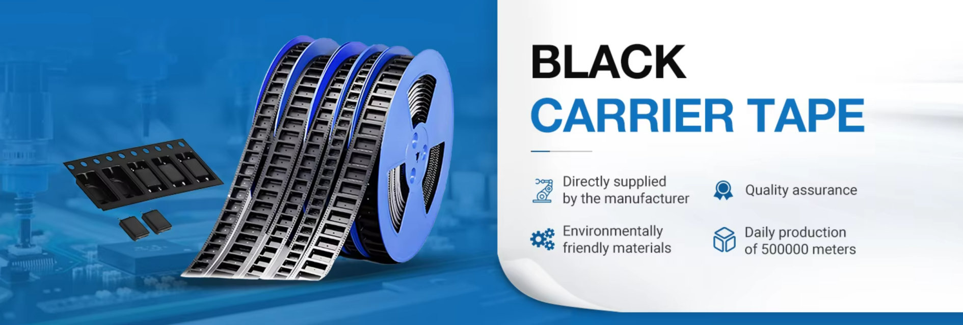
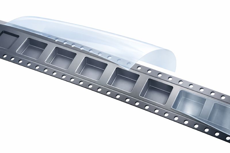
Anti-static carrier tape is a type of embossed or punched carrier tape engineered with ESD-safe properties to prevent the accumulation of static electricity on its surface. It is used in tape and reel packaging to protect sensitive electronic components throughout the supply chain.
Unlike standard plastic carrier tapes, anti-static versions are treated or compounded with materials that control surface resistivity and static behavior.
Key functions include:
- Preventing electrostatic charge buildup
- Reducing risk of ESD damage to components
- Ensuring stable component positioning during transport
- Supporting consistent feeding in SMT machines
It’s important to distinguish between three common ESD classifications:
- Anti-static: Prevents charge generation
- Dissipative: Slowly dissipates charge
- Conductive: Rapidly transfers charge to ground
Anti-static carrier tape is typically used for general semiconductor packaging where moderate ESD protection is sufficient.
Why ESD Protection Is Critical in Semiconductor Packaging
Electrostatic discharge (ESD) occurs when two objects with different electrical potentials come into contact or close proximity, causing a sudden flow of electricity. While often invisible, ESD can severely impact semiconductor components.
There are two major types of ESD damage:
- Catastrophic failure: Immediate and complete component failure
- Latent defects: Hidden damage that reduces long-term reliability
Latent defects are particularly dangerous because components may pass initial testing but fail later in the field, leading to costly recalls or product failures.
In high-reliability industries such as automotive electronics, medical devices, and industrial control systems, even minor ESD damage can result in:
- Reduced yield in SMT assembly
- Increased defect rates
- Warranty claims and brand damage
Compared to these risks, investing in proper anti-static carrier tape is a low-cost but high-impact solution that significantly improves overall product reliability.
Types of Anti-Static Carrier Tape Materials
The performance of anti-static carrier tape largely depends on the material used. Different materials offer varying levels of strength, precision, and ESD protection.
| Material | ESD Type | Advantages | Typical Use |
|---|---|---|---|
| PS (Polystyrene) | Anti-static / dissipative | Cost-effective, easy forming | General IC packaging |
| PET | Dissipative | High strength, dimensional stability | Fine-pitch components |
| PC | Conductive | Superior durability, high precision | Automotive / high-end semiconductors |
Key Considerations:
- PS (Polystyrene): Ideal for standard applications where cost efficiency is important
- PET: Offers better mechanical strength and is suitable for precision components
- PC (Polycarbonate): Used when higher performance and conductivity are required
Selecting the right material depends on both the sensitivity of the component and the requirements of the SMT process.
Key Design Parameters for Anti-Static Carrier Tape
The performance of anti-static carrier tape depends on a combination of material characteristics and structural design. These parameters are typically defined based on component geometry, handling conditions, and compatibility with automated assembly systems.
Surface Resistivity
Surface resistivity is used to describe how the material manages electrostatic charge on its surface. Anti-static carrier tapes are generally produced within a controlled resistivity range, allowing charge accumulation to be reduced under normal handling conditions.
Different applications may require different resistivity levels depending on component sensitivity and environmental factors such as humidity and handling processes.
Pocket Geometry and Tolerances
The pocket structure is designed according to the size and shape of the component. Key considerations include:
- Pocket depth relative to component height
- Clearance to prevent excessive movement
- Edge design to support stable positioning
Tolerances are typically controlled to ensure consistent placement behavior during transport and feeding.
Tape Width and Pitch
Carrier tape dimensions, including width and pocket spacing (pitch), are usually aligned with industry standards such as EIA-481.
Standardized dimensions help ensure compatibility with automated feeders and placement equipment used in SMT processes.
Cover Tape Compatibility
The interaction between carrier tape and cover tape affects how components are retained and released during operation.
Peel characteristics are typically evaluated to maintain a balance between:
- Secure component retention during transport
- Controlled release during feeding
This balance may vary depending on equipment setup and process requirements.
Mechanical Stability
Mechanical properties such as rigidity and dimensional stability influence how the tape behaves during winding, transport, and feeding.
Stable tape structure can help reduce issues such as deformation or misalignment, particularly in high-speed assembly environments.
Static Decay Characteristics
Static decay refers to how quickly an accumulated charge reduces over time. While not always specified in all applications, it may be considered in environments where electrostatic control is critical.
Anti-Static vs Conductive Carrier Tape: What’s the Difference?
Choosing between anti-static and conductive carrier tape depends on the level of ESD protection required.
| Feature | Anti-Static Tape | Conductive Tape |
|---|---|---|
| Function | Prevent charge buildup | Discharge electricity |
| Resistance | Medium (10⁵–10¹¹ Ω) | Low (≤10⁴ Ω) |
| Cost | Lower | Higher |
| Application | Standard ICs | Highly sensitive chips |
Decision Guide:
- Use anti-static tape for most general semiconductor components
- Use conductive tape for highly sensitive devices, such as advanced ICs or automotive-grade semiconductors
While conductive tape offers higher protection, it is often unnecessary for standard applications and increases cost.
Applications in Semiconductor Packaging
Anti-static carrier tape is widely used across different semiconductor packaging scenarios.
Common applications include:
- IC components: QFN, BGA, SOP packages
- LED packaging: Prevents static-induced light degradation
- Automotive semiconductors: Requires higher reliability standards
- High-speed SMT lines: Ensures stable feeding and placement
Each application may require different ESD levels, making proper material and design selection essential.
Common Problems Without Proper Anti-Static Carrier Tape
Using non-ESD-safe or poorly designed carrier tape can lead to serious production and quality issues.
Typical problems include:
- Component sticking or jumping due to static charge
- ESD damage during feeding
- Mis-pick or placement errors in SMT machines
- Increased defect rates and yield loss
These issues not only affect production efficiency but also increase overall manufacturing costs.
How to Choose the Right Anti-Static Carrier Tape Supplier
Selecting the right supplier is just as important as choosing the right material or design.
Key evaluation criteria:
- Material capability: PS, PET, PC options available
- ESD performance testing: Surface resistivity and decay testing
- Custom design capability: Pocket design for specific components
- Standards compliance: EIA-481 compatibility
- Lead time and MOQ: Suitable for your production scale
- Engineering support: Ability to optimize design
Ask these questions before ordering:
- Can you provide ESD test reports?
- Do you support custom tooling?
- How do you control dimensional tolerances?
- What is your typical lead time?
A reliable supplier reduces both technical risks and supply chain uncertainty.
Custom Anti-Static Carrier Tape vs Standard Tape
Choosing between standard and custom carrier tape depends on your application complexity.
Standard Tape:
- Suitable for common components
- Faster lead time
- Lower cost
Custom Tape:
- Required for irregular shapes or tight tolerances
- Optimized for high-speed automation
- Better protection for sensitive components
For most semiconductor manufacturers, custom carrier tape provides better long-term value, especially in high-volume production.
Manufacturing Process of Anti-Static Carrier Tape (Brief Overview)
Understanding the production process helps evaluate supplier capability and quality control.
Typical process:
- Material preparation (ESD-treated plastic sheets)
- Thermoforming / embossing to create pockets
- Punching sprocket holes for indexing
- Surface treatment to achieve anti-static properties
- Inspection and packaging
Precision in each step ensures consistent performance in SMT operations.
FAQs
1. What is the difference between anti-static and ESD-safe carrier tape?
Anti-static tape prevents charge buildup, while ESD-safe may include both anti-static and conductive properties.
2. What resistance range is considered anti-static?
Typically between 10⁵ and 10¹¹ ohms.
3. Is anti-static carrier tape enough for all semiconductor components?
No. Highly sensitive components may require conductive carrier tape.
4. How is ESD performance tested?
Through surface resistivity measurement and static decay testing.
5. Can anti-static carrier tape be customized?
Yes, most manufacturers offer custom pocket design and material options.
Conclusion
Anti-static carrier tape is commonly used in semiconductor packaging to help manage electrostatic conditions while supporting component handling and automated assembly processes. Its effectiveness is influenced by multiple factors, including material selection, structural design, and compatibility with specific production environments.
In practical applications, selecting an appropriate carrier tape solution often involves balancing electrical characteristics, mechanical stability, and process requirements. Differences in component sensitivity, equipment setup, and operating conditions may all affect the final choice.
Rather than relying on a single specification, it is generally more effective to evaluate carrier tape options based on actual use scenarios, including feeding performance, packaging consistency, and overall process compatibility.
For applications with more specific requirements, working with a supplier that can provide technical support and design adjustments may help improve alignment between packaging solutions and production needs.



 Emial
Emial John Mr