



Tape and Reel Packaging for Semiconductor Devices: Complete Guide to IC and Chip Packaging
Semiconductor devices are smaller, more fragile, and more sensitive to static electricity than ever before. Whether you are packaging integrated circuits, MOSFETs, sensors, or power devices, improper handling can easily lead to bent leads, cracked packages, ESD damage, or pick-and-place failures.
That is why tape and reel packaging has become the standard method for shipping and feeding semiconductor components into SMT assembly lines. By combining carrier tape, cover tape, and plastic reels, manufacturers can protect devices during transport while ensuring fast, accurate automated placement.
In this guide, you will learn how semiconductor tape and reel packaging works, which materials and standards matter most, and how to choose the right solution for different semiconductor packages.

What Is Tape and Reel Packaging for Semiconductor Devices?
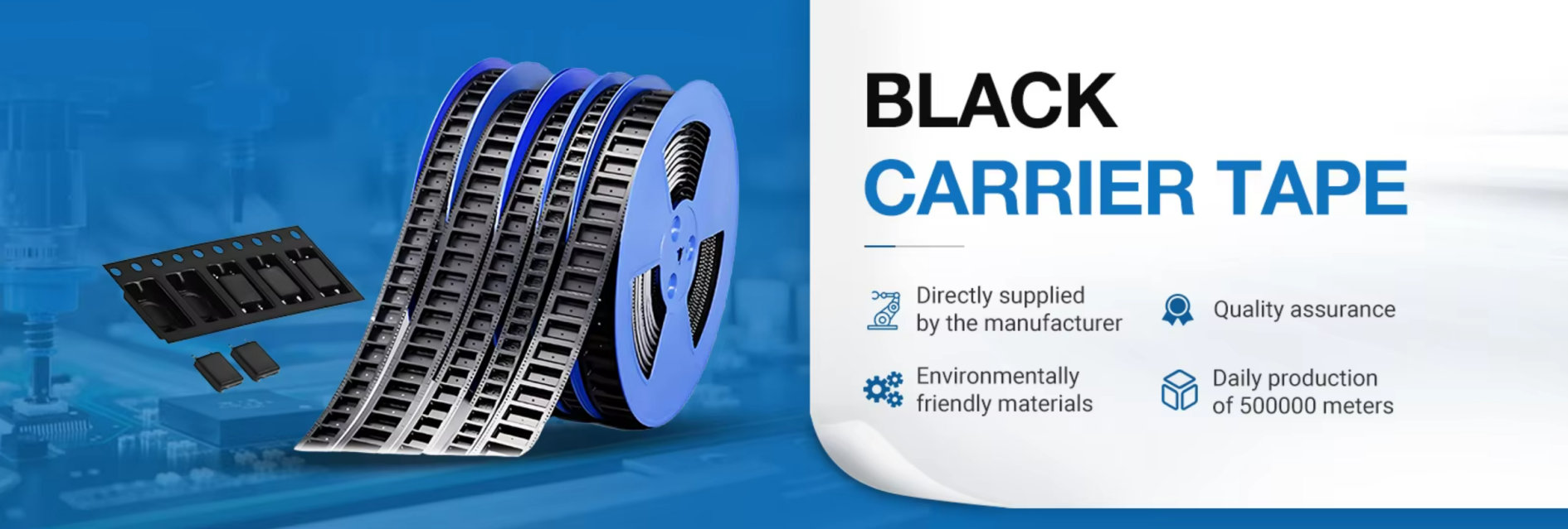
Tape and reel packaging is a packaging system used to store, protect, and feed semiconductor devices into automated SMT equipment.
The system contains three main parts:
-
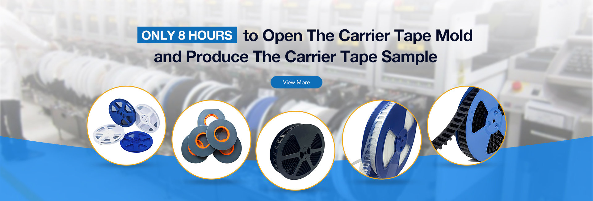
Carrier tape with precisely formed pockets
-
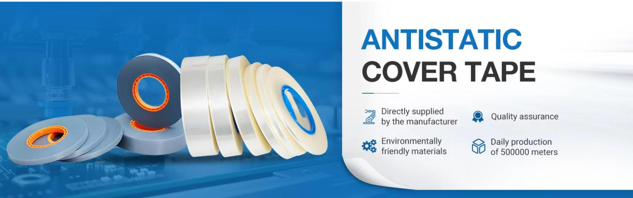
Cover tape that seals the devices into those pockets
-
A plastic reel that holds the tape for shipment and machine feeding
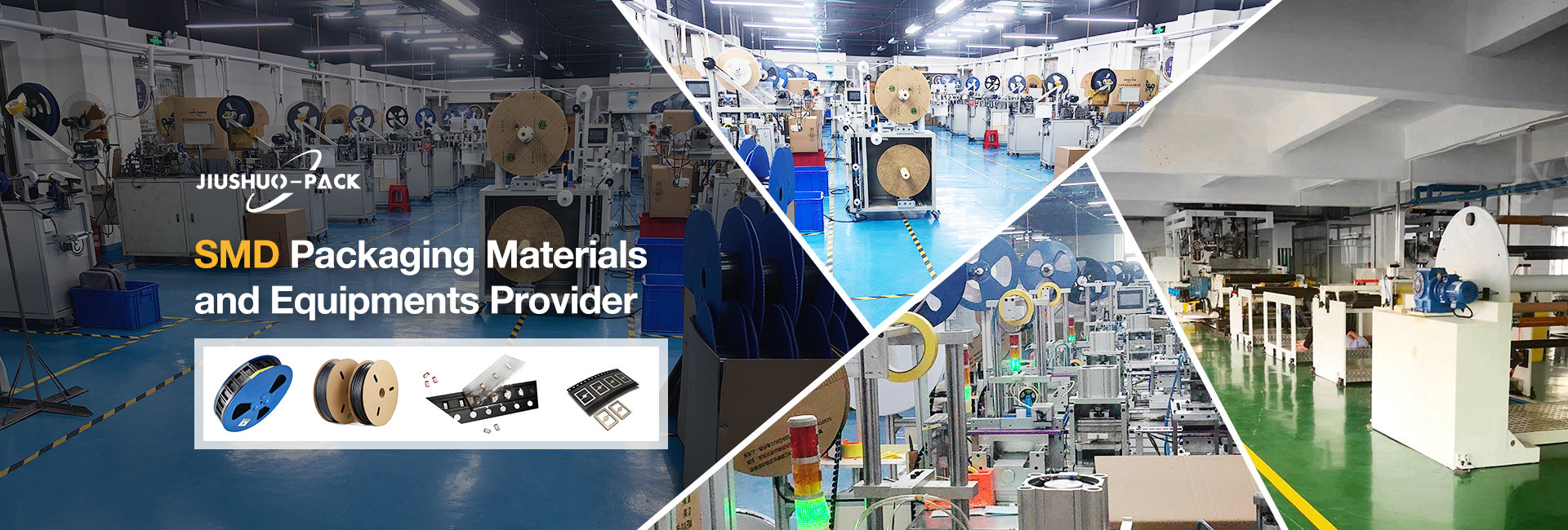
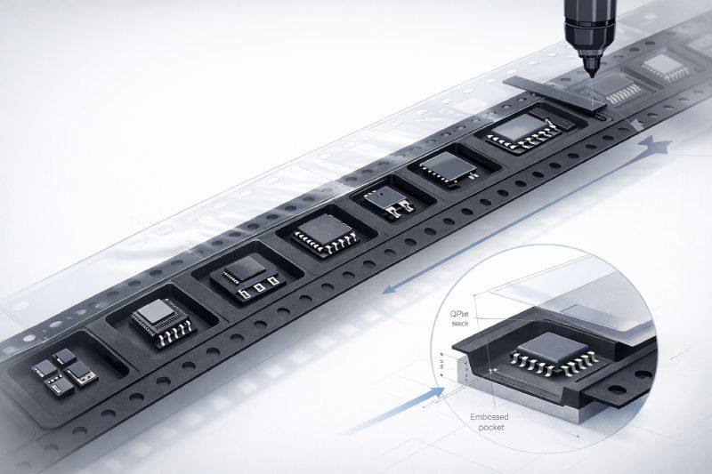
Each semiconductor device is placed into an individual pocket inside the carrier tape. After the cover tape is sealed, the tape is wound onto a reel. The reel can then be loaded directly into an SMT feeder, allowing the assembly machine to automatically advance the tape and pick each component.
Tape and reel packaging is widely used for:
-
Integrated circuits (ICs)
-
Transistors
-
Diodes
-
LEDs
-
Memory chips
-
Sensors
-
MOSFETs
-
QFN, BGA, SOP, SOT, and DFN packages
Compared with bulk packaging or trays, tape and reel packaging provides better component protection and much higher production efficiency. It also reduces manual handling, which lowers the risk of contamination and damage.
Why Semiconductor Devices Need Specialized Tape and Reel Packaging
Semiconductor devices are not all packaged the same way. A tiny DFN package and a large BGA package have very different handling requirements. Semiconductor tape and reel packaging must therefore be designed specifically for the size, weight, sensitivity, and orientation of the device.
Protection Against Physical Damage
Many semiconductor packages include delicate leads, exposed pads, or thin plastic housings. During transportation, even small amounts of movement can damage the device.
A properly designed carrier tape pocket prevents components from moving, rotating, or colliding with each other. This is especially important for:
-
Fine-pitch IC packages
-
Thin QFN or DFN devices
-
Large power semiconductors
-
Fragile MEMS sensors
Without proper pocket dimensions, semiconductor devices may tilt inside the cavity, leading to bent leads, cracked edges, or feeding problems.
ESD and Anti-Static Protection
Electrostatic discharge is one of the biggest risks in semiconductor packaging. A small static discharge that is invisible to the human body can permanently damage an IC.
For this reason, semiconductor tape and reel packaging often uses:
-
Anti-static carrier tape
-
Conductive carrier tape
-
ESD-safe cover tape
-
Anti-static reels and packaging bags
Common materials such as PS, PC, and PET can be manufactured in anti-static or conductive grades. The correct material depends on how sensitive the semiconductor device is and how it will be handled during shipping and assembly.
Moisture and Contamination Control
Semiconductor packages must remain clean before they enter the SMT process. Dust, moisture, and contamination can reduce soldering quality or affect device performance.
The cover tape seals the component inside the carrier tape pocket, helping keep contaminants away. For highly sensitive devices, the completed reel is often packed inside a moisture barrier bag together with desiccant and humidity indicator cards.
Stable High-Speed Feeding
Modern SMT lines operate at very high speeds. If the tape pitch, pocket position, or reel dimensions are incorrect, the feeder may jam or mis-pick components.
Accurate tape and reel design ensures:
-
Smooth tape advancement
-
Stable component orientation
-
Reliable pick-and-place performance
-
Lower feeder downtime
A poorly designed tape may save money initially, but it often leads to rejected boards, lost production time, and damaged semiconductor devices.
Main Components of Semiconductor Tape and Reel Packaging
Carrier Tape
Carrier tape is the most important part of the packaging system. It contains the pockets that hold the semiconductor device.
There are two main types of carrier tape:
-
Embossed carrier tape
-
Punched carrier tape
Embossed carrier tape is the most common choice for semiconductor devices because it allows custom pocket shapes and depths. It is ideal for ICs, QFNs, BGAs, and other precision components.
Punched carrier tape is usually used for simpler and flatter devices where the cavity can be cut directly into the tape.
The most common carrier tape materials are:
-
Polystyrene (PS)
-
Polycarbonate (PC)
-
PET
PS is economical and widely used for standard semiconductor devices. PC offers better dimensional stability and is often used for more demanding packages. PET is valued for its durability and anti-static performance.
For ESD-sensitive components, conductive or anti-static versions of these materials are normally required.
Cover Tape
Cover tape seals the semiconductor devices inside the carrier tape pocket.
There are two main cover tape options:
-
Heat-activated cover tape
-
Pressure-sensitive cover tape
Heat-activated cover tape is common in semiconductor packaging because it provides a strong, stable seal and excellent protection during transport.
Pressure-sensitive cover tape is easier to apply and is often used for smaller production runs or devices that require easier opening.
The cover tape must have the correct peel force. If the peel force is too low, the components may escape from the pockets during shipment. If the peel force is too high, the SMT feeder may struggle to remove the cover tape, causing jams or part damage.
Plastic Reel
After sealing, the carrier tape is wound onto a plastic reel. The reel keeps the tape organized and compatible with SMT feeders.
Typical reel diameters include:
-
7-inch reel
-
13-inch reel
-
15-inch reel
Smaller reels are usually used for low-volume production or narrow tape widths. Larger reels are preferred for high-volume semiconductor manufacturing because they hold more components and reduce machine downtime.
The reel size must match the customer’s feeder system. Using the wrong reel diameter can cause loading problems or production delays.
Leader and Trailer Tape
Leader tape is the empty section at the beginning of the reel. Trailer tape is the empty section at the end.
These empty sections allow the SMT feeder to load and unload properly without wasting packaged semiconductor devices. They also improve machine setup and reduce the chance of losing components during the first or last part of the reel.
How the Semiconductor Tape and Reel Packaging Process Works
Step 1: Device Inspection and Orientation
Before packaging begins, semiconductor devices are inspected for defects and checked for proper orientation.
Every component must face the correct direction inside the carrier tape pocket. The orientation is important because SMT machines rely on a consistent position when picking the device.
For example, the pin-1 location of an IC may need to face a specific side of the tape. If the orientation is incorrect, the component may be placed incorrectly onto the PCB.
Step 2: Loading Devices into Carrier Tape
The semiconductor devices are then loaded into the carrier tape pockets.
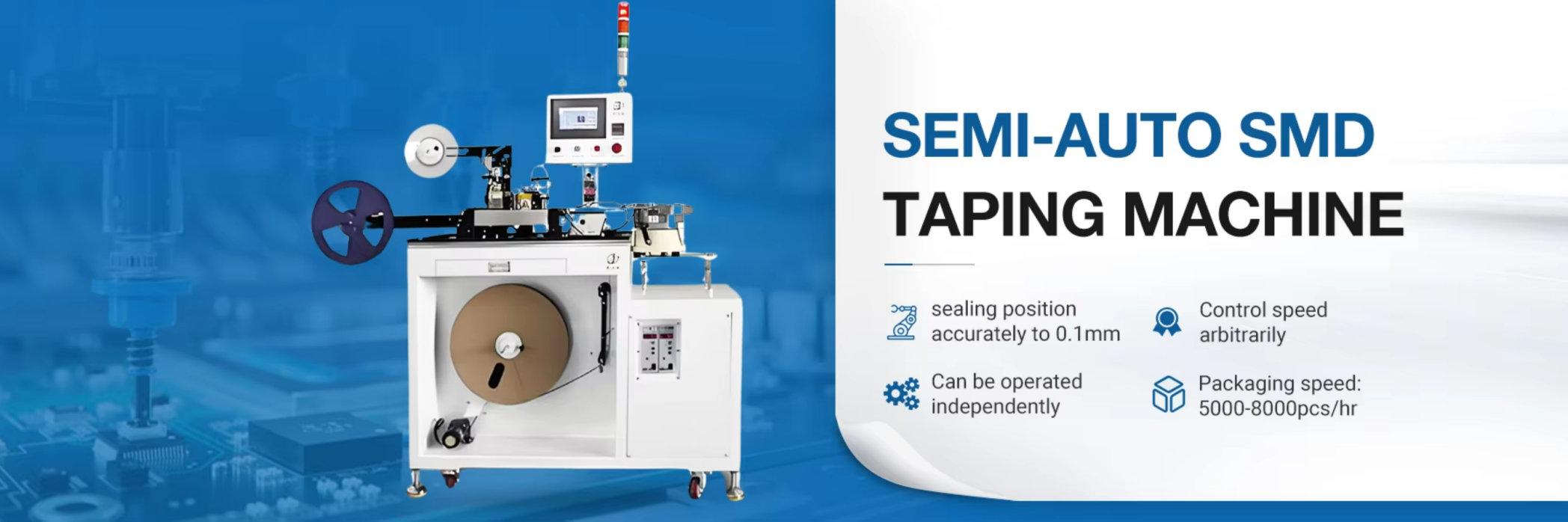
In most cases, this is done using automated tape and reel machines. The machine places one component into each pocket while maintaining the required orientation and pitch.
Custom pocket dimensions are often used to ensure the semiconductor device fits tightly without being damaged.
Step 3: Cover Tape Sealing
Once the devices are loaded, the cover tape is applied.
For heat-activated cover tape, the sealing machine uses carefully controlled temperature, pressure, and speed. These parameters are important because too much heat may damage the device or deform the carrier tape, while too little heat may result in poor sealing.
Step 4: Reeling and Final Inspection
After sealing, the tape is wound onto a reel.
Before shipment, the finished reel is inspected for:
-
Correct device orientation
-
Missing or damaged components
-
Pocket alignment
-
Tape pitch accuracy
-
Cover tape peel force
-
Reel dimensions
Many semiconductor packaging suppliers also perform sample feeder tests to confirm the reel works correctly in SMT equipment.
Step 5: Final Packaging and Shipment
The completed reel is packed for transport.
For ESD-sensitive semiconductor devices, the reel is usually sealed inside:
-
Anti-static bag
-
Moisture barrier bag
-
Vacuum packaging
-
Dry pack with desiccant
This final layer of protection helps maintain device quality until the reel reaches the customer’s production line.
Semiconductor Package Types and Their Packaging Requirements
Different semiconductor packages require different tape and reel designs.
| Package Type | Typical Tape Width | Common Challenge |
|---|---|---|
| SOT / SOD | 8 mm | Very small pocket size and precise orientation |
| QFN / DFN | 8–12 mm | Preventing device tilt and maintaining flatness |
| SOP / SOIC | 12–16 mm | Protecting leads from bending |
| BGA / LGA | 16–32 mm | Large pocket depth and stable positioning |
| Power Modules | 24–56 mm | Heavy weight and deep cavity design |
| MEMS Sensors | Custom | Fragile structure and strict orientation control |
Small Surface-Mount Packages
Small semiconductor packages such as SOT, DFN, and QFN often use narrow 8 mm carrier tape.
Because these devices are lightweight and compact, the pocket dimensions must be extremely accurate. Even a small amount of extra space can allow the component to rotate or move.
Large and Complex Packages
Packages such as BGA, QFP, and power semiconductors require larger tape widths and deeper pockets.
These devices are heavier and often need stronger carrier tape materials to maintain stability during transport.
Fragile and Custom-Shaped Devices
MEMS sensors, optical sensors, and irregular semiconductor packages often require custom embossed carrier tape.
A standard pocket may not support these devices properly. Custom cavity shapes help reduce stress on fragile areas while keeping the device securely in place.
Understanding EIA-481 Standards
EIA-481 is the international standard used for tape and reel packaging in electronics and semiconductor manufacturing.
The standard defines critical packaging dimensions and requirements, including:
-
Tape width
-
Pocket pitch
-
Pocket depth
-
Sprocket hole position
-
Reel dimensions
-
Component orientation
Following EIA-481 is important because it ensures the reel can run correctly in SMT equipment worldwide.
If a semiconductor tape and reel design does not follow the standard, the feeder may not align properly with the sprocket holes or pocket positions. This can lead to mis-picks, machine stoppages, and lost production time.
EIA-481 compliance is especially important when:
-
Supplying multiple customers
-
Shipping internationally
-
Using different SMT feeder brands
-
Packaging custom semiconductor devices
When evaluating a packaging supplier, always confirm that the carrier tape and reel design meets EIA-481 requirements.
Common Problems in Semiconductor Tape and Reel Packaging
Incorrect Pocket Size
If the pocket is too large, the semiconductor device may move or rotate inside the cavity. If the pocket is too small, the device may become damaged during loading.
The best solution is to create a pocket based on the actual dimensions of the semiconductor package.
Wrong Component Orientation
Incorrect orientation is one of the most common causes of SMT assembly errors.
Before mass production, always confirm the orientation with the customer’s drawing or feeder requirement.
Poor Cover Tape Peel Force
Weak peel force can allow components to escape from the tape during transport. Excessive peel force can create feeder problems.
A reliable supplier should test peel force before shipment.
ESD Failure
Using standard carrier tape for an ESD-sensitive semiconductor device can cause hidden electrical damage.
Always choose conductive or anti-static materials when packaging ICs, MOSFETs, memory devices, or other sensitive components.
Reel Compatibility Issues
Not all SMT feeders accept the same reel size.
Before production begins, verify:
-
Reel diameter
-
Tape width
-
Hub size
-
Direction of reel winding
This prevents costly delays after the reels arrive at the assembly line.
Need help choosing the right semiconductor tape and reel design? Sharing your device drawing or package dimensions is often the fastest way to receive an accurate recommendation.
How to Choose the Right Tape and Reel Packaging Supplier
Not every tape and reel supplier has experience with semiconductor devices.
When selecting a supplier, look for the following:
-
Experience with IC, QFN, BGA, and ESD-sensitive packages
-
Ability to design custom embossed carrier tape
-
Availability of anti-static and conductive materials
-
EIA-481-compliant production
-
Cover tape peel force testing
-
Sample validation before mass production
A good semiconductor packaging supplier should also be able to review your device drawing and recommend:
-
The best carrier tape material
-
Pocket dimensions
-
Correct tape width
-
Suitable reel size
-
Appropriate cover tape type
Production capacity and lead time are also important. Semiconductor manufacturers often operate on tight schedules, so the packaging supplier must be able to support both sample quantities and high-volume production.
Why Custom Tape and Reel Packaging Is Often Necessary
Many semiconductor devices do not fit standard carrier tape pockets.
For example, a MEMS sensor may require a unique cavity shape to protect delicate structures, while a large power semiconductor may need a deeper pocket and stronger material.
Custom tape and reel packaging provides several advantages:
-
Better protection during shipping
-
Improved feeder performance
-
Lower risk of part damage
-
More stable component orientation
-
Reduced SMT defects
Although custom tooling may slightly increase the initial cost, it often reduces total production cost by preventing feeder downtime and rejected boards.
For semiconductor manufacturers, custom embossed carrier tape is often the safest and most reliable solution.
Conclusion
Tape and reel packaging plays a critical role in semiconductor manufacturing. It protects fragile devices during transport, prevents ESD and contamination, and supports high-speed automated SMT assembly.
The right solution depends on choosing the correct carrier tape material, pocket design, cover tape, reel size, and EIA-481-compliant dimensions.
For many ICs, sensors, and advanced semiconductor packages, custom tape and reel packaging provides the best balance of protection and feeder reliability.
If you are packaging a new semiconductor device, the best next step is to send your package drawing or dimensions to an experienced tape and reel supplier. A custom recommendation or sample reel can help you avoid costly production issues before mass manufacturing begins.



 Emial
Emial John Mr